
Matching a GAGG Scintillator Array to a SiPM
When specifying a GAGG scintillator array for SiPM readout, start with the sensor drawing. Crystal pixel width, assembled pixel pitch and SiPM channel spacing describe different dimensions. An array can have the correct number of pixels and still be misaligned with the photosensor.
This guide explains how to calculate pitch, account for reflector and bonding layers, and prepare a drawing for a custom GAGG(Ce) scintillator array.
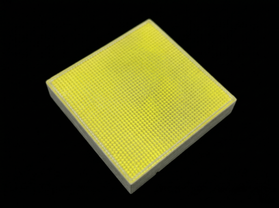
Crystal Pixel Size, Channel Pitch and Microcell Pitch
- Crystal pixel size: the width and length of one GAGG element, excluding the separator between neighbouring elements.
- Array pixel pitch: the centre-to-centre distance between adjacent crystal elements in the finished assembly.
- SiPM channel pitch: the centre-to-centre distance between neighbouring readout channels. Check the package drawing, not only the active-area specification.
- SiPM microcell pitch: a much smaller dimension within each channel. It does not specify the spacing required between crystal elements.
For example, the Hamamatsu S13361-3050 series datasheet lists a 3 × 3 mm photosensitive area per channel and a 50 µm microcell pitch. These are different scales. Use the dimensional outline to establish channel spacing before specifying the GAGG array.
How to Calculate GAGG Array Pixel Pitch
For equal-width crystal pixels separated by one shared layer, the nominal relationship is:
Pixel pitch = crystal pixel width + finished separator thickness.
The separator dimension must include the complete space between the crystals, including reflector and adhesive where applicable. A reflector film’s nominal thickness alone may not equal the finished gap.
For direct one-to-one coupling, compare the assembled crystal pitch with the SiPM channel pitch in both directions. If the design uses a light guide or distributes light across multiple sensor channels, define that readout arrangement separately.
Worked Example: An 8 × 8 GAGG Array
The following is a geometry example, not a standard stock configuration or a compatibility guarantee for a particular sensor.
| Drawing item | Example value |
|---|---|
| Crystal pixel width and length | 3.0 × 3.0 mm |
| Finished separator between pixels | 0.2 mm |
| Centre-to-centre pitch | 3.2 mm in both directions |
| Pixel count | 8 × 8 |
| Span before outer edge layers | 25.4 × 25.4 mm |
| Crystal thickness | Specified separately for the detector requirement |
Eight crystals have seven internal separators. The span along either axis is therefore:
8 × 3.0 + 7 × 0.2 = 25.4 mm.
If an outer layer adds 0.1 mm on each side, the finished size along that axis becomes 25.6 mm. Without that edge-layer assumption, multiplying eight pixels by the 3.2 mm pitch would give the wrong outside dimension.
For a uniform row, use outside dimension = N × w + (N − 1) × s + left edge layer + right edge layer, where N is the pixel count, w is the crystal width and s is the finished internal separator thickness. Apply the calculation independently to each axis.
What to Show on the Array Drawing
- Top view: rows, columns, crystal pixel dimensions, pitch in X and Y, and finished outside dimensions.
- Side view: crystal thickness, any cover or light guide, and the optical coupling face.
- Optical treatment: polished or other required surfaces, internal reflector, outer wrapping and any intentionally open faces.
- Alignment: the reference edge, first pixel centre, sensor orientation and mechanical mounting arrangement.
- Tolerances: individual pixel dimensions, assembled pitch and total dimensions. State the allowable registration error for the complete array.
Send the SiPM model and dimensional drawing with the crystal drawing. A small pitch difference accumulates across successive pixels, so checking only the first channel is insufficient.
Reflectors and Optical Coupling
Review the reflector and bonding method together with the required light collection and pixel separation. More collected light and less optical sharing are separate design goals; establish which matters most for the intended readout.
Specify whether the array couples directly to the sensor window or through a light guide. Include the coupling material and intended interface thickness in the assembly review. Final detector performance also depends on the selected GAGG grade, sensor spectral response, electronics and measurement conditions.
Request a Custom GAGG Array Quotation
For an initial review, provide the SiPM model, application, pixel count, crystal pixel dimensions, target pitch, finished separator thickness, reflector and adhesive requirements, crystal thickness, finished outside dimensions, optical treatment, quantity and drawings. If the geometry is not final, send the sensor drawing and the dimensions already known.
Review the GAGG(Ce) array product page for available design options. For a single-piece crystal rather than a pixelated assembly, see our GAGG(Ce) scintillation crystals.
Send your requirements to sales@atrscintillator.com, or use the online inquiry form. The proposed geometry, material grade and acceptance criteria are confirmed during quotation.