Single-crystal wafers and substrates

Crystal Wafers and Substrates for Photonics, SAW and Electro-Optic Devices

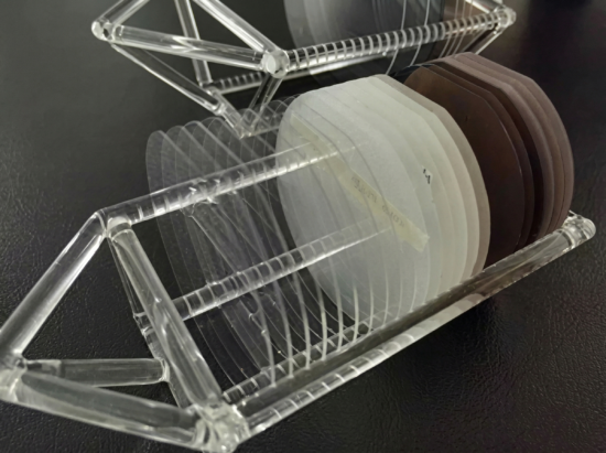
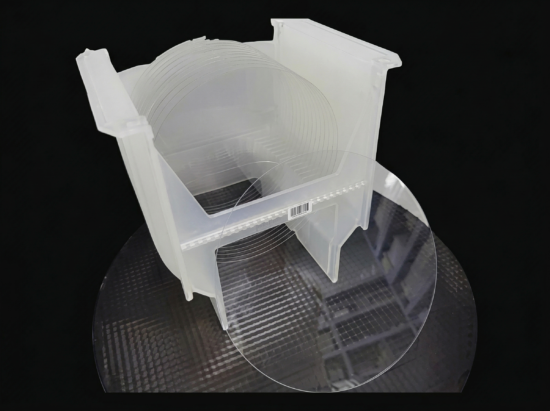
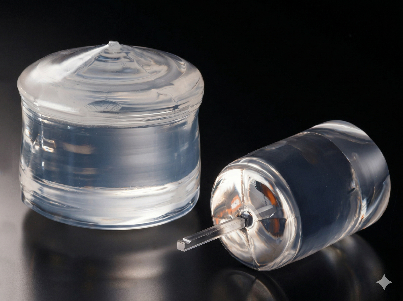
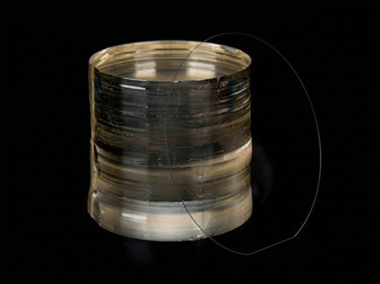
ATR Crystal supplies optical-grade crystal wafers and single-crystal substrates for photonics, electro-optic modulators, SAW devices, nonlinear optics and precision optical components. Available materials include lithium niobate wafers (LiNbO3), lithium tantalate wafers (LiTaO3), quartz single-crystal wafers and other drawing-defined substrates. Cut orientation, diameter, thickness, TTV, bow, warp, SSP or DSP polishing, surface roughness, edge criteria and inspection requirements can be reviewed according to the device process.

What can be customized?

  • LiNbO3, LiTaO3 and quartz single-crystal wafer options
  • X-cut, Y-cut, Z-cut, rotated cuts and drawing-defined orientation
  • Diameter, thickness, TTV, bow, warp and edge requirements
  • SSP, DSP and lapped surfaces with agreed inspection criteria

Selection guide

Crystal Wafer and Substrate Selection Guide

MaterialTypical roleCommon applications
LiNbO3 waferElectro-optic, nonlinear-optical and piezoelectric single-crystal substrate.Modulators, waveguides, PPLN research, SAW devices and photonics.
LiTaO3 waferPiezoelectric, pyroelectric and electro-optic substrate.SAW filters, sensors, infrared devices and optical components.
Quartz single-crystal waferStable piezoelectric and optical substrate with drawing-defined crystal orientation.Frequency-control devices, SAW components, sensors and precision optics.

Available products

Crystal Wafer and Substrate Products

Optical Grade Quartz Single Crystal Wafers

Optical Grade Quartz Single Crystal Wafers

Single crystal quartz wafers are synthetic quartz substrates used for SAW filters, resonators, frequency-control devices, optical low-pass filters, waveplates, polarizing optics, sensors, and precision…

View Details
Optical Grade Lithium Tantalate Wafers

Optical Grade Lithium Tantalate Wafers

Lithium tantalate wafers, also known as LiTaO3 wafers, are single crystal substrates used for SAW devices, RF filters, pyroelectric infrared detectors, electro-optic components, nonlinear…

View Details
Optical Grade Lithium Niobate Wafers

Optical Grade Lithium Niobate Wafers

Lithium niobate wafers, also known as LiNbO3 wafers, are optical and electro-optic substrates used when a device requires strong electro-optic response, useful nonlinear optical…

View Details

Manufacturing support

Custom Crystal Wafer and Substrate Capabilities

Crystallographic specification

Cut orientation, orientation tolerance, primary flat direction and drawing requirements can be reviewed before quotation.

Wafer geometry

Diameter, thickness, TTV, bow, warp, edge profile and handling requirements should be defined according to the downstream process.

Surface and inspection

SSP, DSP or lapped surfaces can be discussed with roughness, visual defect, particle and packing requirements.

Need a custom crystal wafer and substrate product?

Send material, size, quantity, surface treatment and application requirements. Drawings are recommended for custom geometries, arrays and assemblies.

Online Quotation Request

FAQ

Crystal Wafer and Substrate Selection Questions

What information is needed for a wafer quote?

Please provide material grade, dopant, cut, diameter, thickness, TTV, bow, warp, polishing type, roughness, edge criteria, quantity and inspection requirements.

What is the difference between optical-grade and SAW-grade wafers?

Optical-grade projects emphasize optical quality and surface finish, while SAW-grade wafers also require application-specific crystal orientation, flat direction and acoustic-device geometry.

Can custom crystal orientations be reviewed?

Yes. Rotated cuts and drawing-defined orientations can be reviewed with orientation tolerance and reference-flat requirements.