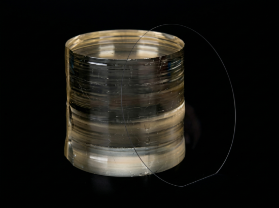
The cut of a lithium niobate wafer identifies which crystal axis is perpendicular to its main surface. X-cut, Y-cut and Z-cut LiNbO3 wafers have the X, Y and Z axes normal to that surface, respectively. Select the orientation around your optical propagation direction, electric-field arrangement and fabrication process, then specify the flat direction and tolerances on the drawing.
A complete wafer enquiry also specifies orientation tolerance, primary-flat direction, material grade, thickness and surface finish. Identify +Z and −Z faces when polarity matters. For a rotated cut, give the angle and reference convention; a cut label alone does not define the complete optical or fabrication geometry.
What X-cut, Y-cut and Z-cut actually mean
The cut identifies the crystallographic axis perpendicular to the main wafer surface:
- X-cut: the surface normal is along the crystal X-axis.
- Y-cut: the surface normal is along the crystal Y-axis.
- Z-cut: the surface normal is along the crystal Z-axis, which is also the optical and ferroelectric polar axis.
This definition is simple, but it does not describe the whole device. The direction of light propagation, acoustic propagation, electrodes, periodic domains and wafer flats may all lie within the wafer plane. Those directions must be defined separately when they affect performance.
A useful way to read a drawing is to ask two questions: which axis points out of the wafer, and which axis is used as the in-plane reference? If the drawing answers only the first question, the supplier may still need clarification before cutting or marking the wafer.
Quick comparison of the three principal cuts
| Cut | Surface normal | Important design point | What to confirm on the RFQ |
|---|---|---|---|
| X-cut | X-axis | The Z-axis lies in the wafer plane, which can be useful when the device needs an in-plane relationship between the optical field and the polar axis. | In-plane Z direction, propagation direction, electrode geometry and flat reference. |
| Y-cut | Y-axis | Used in bulk optical wafers and as the starting convention for several rotated acoustic cuts. | Whether it is a principal Y-cut or a rotated Y-cut, plus the rotation angle and propagation convention. |
| Z-cut | Z-axis | The polar axis is normal to the wafer surface, so the two major faces are not interchangeable when polarity matters. | Identification of +Z and −Z faces, polished side, flat direction and any poling requirement. |
No cut is universally better. The useful orientation is the one that places the relevant tensor component and field direction correctly for the device. A quotation based only on the lowest wafer price can be misleading if the orientation later forces a change in electrodes, waveguide layout or processing.
Choosing a cut for electro-optic devices
Electro-optic performance depends on more than the material’s headline coefficient. The result also depends on optical polarization, propagation direction and the direction of the applied electric field. An X-cut and a Z-cut modulator can therefore use different electrode and waveguide arrangements even though both are made from lithium niobate.
For a custom bulk wafer or substrate, do not select the cut from the application name alone. “Phase modulator” or “electro-optic switch” does not define the geometry. The RFQ should show the beam direction, polarization and electrode field direction. If the device layout is confidential, an axis diagram without the complete system drawing is often enough for the wafer manufacturer to verify orientation.
The same caution applies when moving a design between bulk LiNbO3 and thin-film lithium niobate. The common cut options may have the same names, but film thickness, waveguide confinement and electrode placement change how the crystal axes are used.
Z-cut wafers, polarity and periodic poling
LiNbO3 is ferroelectric, so the positive and negative Z directions are physically meaningful. On a Z-cut wafer, one major face corresponds to +Z and the opposite face to −Z. Double-side polishing does not remove this distinction.
If surface treatment, domain inversion, bonding or electrode processing depends on polarity, ask for the faces to be identified on the packaging, inspection record or wafer marking. Writing only “Z-cut DSP” may not be sufficient.
For periodically poled lithium niobate, the drawing should define the poling direction, grating direction, period, aperture and optical propagation direction. “PPLN wafer” is not a complete orientation specification. Periodic poling works by reversing ferroelectric domains, and the usable nonlinear interaction also depends on how the optical beams travel relative to those domains.
Why rotated Y-cut needs an angle and a convention
SAW and other acoustic devices often use rotated cuts rather than a principal X-, Y- or Z-cut. Specifications such as 128° Y-cut, 127.86° rotated Y-cut or Y-135 describe a controlled rotation from a crystallographic reference. The exact notation should not be shortened to “Y-cut” during purchasing.
For a rotated cut, confirm:
- the nominal rotation angle;
- the axis about which the rotation is made;
- the positive or negative rotation convention;
- the intended acoustic propagation direction;
- the orientation tolerance and measurement method;
- the relationship between the primary flat and crystal axes.
Two drawings can show the same angle but use different viewing or rotation conventions. An axis sketch is safer than relying on a short material description copied from an older purchase order.
Orientation tolerance is not surface flatness
Orientation tolerance describes how accurately the polished wafer plane follows the requested crystallographic plane. Surface flatness describes the geometric variation of the finished surface. TTV, bow and warp are separate measurements again.
This distinction is important in quotations. A wafer may have excellent surface flatness but still be cut outside the required crystallographic orientation tolerance. Conversely, a tightly oriented wafer can fail a demanding bonding or lithography process if TTV and bow are not controlled.
When comparing quotations, check that each supplier is responding to the same list of requirements:
- cut orientation and orientation tolerance;
- diameter, thickness and thickness tolerance;
- SSP or DSP surface processing;
- TTV, bow, warp and surface roughness;
- primary flat length and axis direction;
- +Z/−Z identification where required;
- edge exclusion, chips, scratches and inspection method.
These items are reviewed in more detail on our optical grade lithium niobate wafer page.
A practical LiNbO3 wafer RFQ example
The following format is more useful than writing only “2-inch Z-cut LiNbO3 wafer.” The values are an example of RFQ structure, not a universal specification:
| Material | Congruent LiNbO3, undoped |
|---|---|
| Cut | Z-cut, orientation tolerance to be stated |
| Polarity | Identify +Z and −Z faces |
| Diameter | 50.8 mm |
| Thickness | 0.50 mm, tolerance to be agreed |
| Surface | Double-side polished |
| Flat | Primary flat direction shown on drawing |
| Geometry | TTV, bow and warp limits stated separately |
| Inspection | Orientation and surface inspection report required |
| Quantity | Prototype and production quantities listed separately |
If the application is electro-optic, add the beam, polarization and electric-field directions. If it is acoustic, add the propagation direction and rotated-cut convention. If it is nonlinear optical, add the wavelength combination, propagation direction and poling details.
Common ordering mistakes
Copying the cut but omitting the flat direction
The supplier knows which plane to polish but not how the wafer should be aligned in downstream equipment. This can lead to an unnecessary clarification round or an incorrectly marked wafer.
Treating both sides of a Z-cut wafer as equivalent
Both sides may meet the same polish specification, but +Z and −Z polarity can still matter for processing. Request face identification when it affects the application.
Ordering a rotated cut as standard Y-cut
For acoustic devices, the missing rotation angle can change the intended wave mode and device response. Keep the complete notation in the RFQ and purchase order.
Using the application name as the orientation specification
“For a modulator,” “for PPLN” or “for SAW” is useful context, but it does not replace an axis definition. Different device geometries can use different cuts within the same application family.
What to send before requesting a quotation
Send the material grade, dopant, cut, orientation tolerance, diameter, thickness, polish type, TTV, bow, warp, roughness, flat direction, polarity marking, quantity and drawing. Also identify whether the requirement is for a bulk wafer, a processed optical substrate or a thin-film platform.
For a wider discussion of material grade, polishing and wafer geometry, see our lithium niobate applications and specification guide. Related substrate options are listed in the crystal wafer and substrate category. If the project is primarily acoustic, it may also be useful to compare LiNbO3 and LiTaO3 wafer options before fixing the material.
Frequently asked questions
Is Z-cut always the correct choice for optical applications?
No. The correct cut depends on propagation direction, polarization, electric-field direction and the device architecture. Optical application alone does not determine the cut.
Does DSP mean the two faces are interchangeable?
No. DSP means both major surfaces are polished. On Z-cut LiNbO3, the two sides still correspond to opposite polar directions.
Is 128° Y-cut the same as standard Y-cut?
No. It is a rotated cut and should be ordered with the complete angle, rotation convention, propagation direction and tolerance.
Should the primary flat be included on the drawing?
Yes. Define the flat length and its relationship to the crystal axes. This helps the wafer supplier and the downstream device process use the same orientation reference.