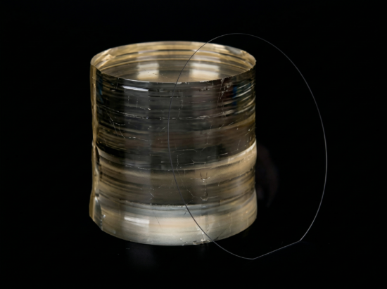
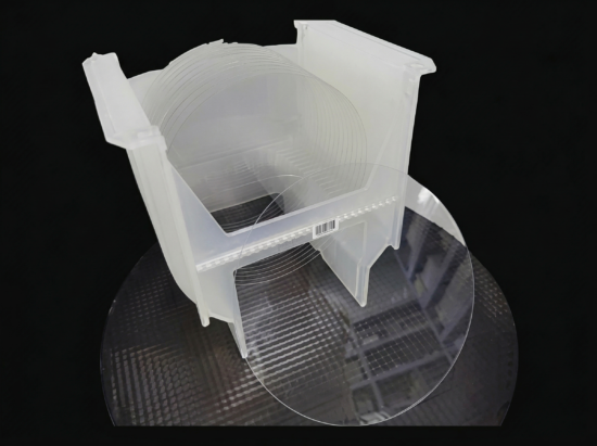
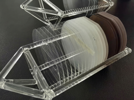
Optical Grade Lithium Niobate Wafers
At Atr Crystal, we offer a comprehensive range of optical-grade Lithium Niobate (LiNbO3) wafers in various sizes and thicknesses. Our wafer diameters range from 2 inches to 4 inches, with customizable thicknesses tailored to your specific requirements (typically 0.18 mm and above). Available crystallographic orientations include X-cut, Y-cut, and Z-cut. In addition to standard Congruent Lithium Niobate (CLN) and Near-Stoichiometric Lithium Niobate (SLN), we also provide specialized doped variants, including Tm-, Pr-, Er-, Fe-, and MgO-doped LiNbO3 wafers to suit diverse application needs.
Product Category:
Crystal Wafer and Substrate
Application of Optical Grade Lithium Niobate Wafers
- Optic Isolators
- Periodically poled lithium niobate (PPLN) waveguides
- EO Phase Modulators
- Optical Modulator
- Electro-optic Q-switches
Advantages of Optical Grade LiNbO3 Wafer
- Stable mechanical properties
- Good machinability
- Heat and corrosion resistance
- High electro-optic and high nonlinear optic coefficients
Ability of Optical Grade Lithium Niobate Wafers
- Diameter: 2”, 3”, 4”
- Orientations: X, Y, Z etc.
- Thickness: 0.25mm, 0.5 mm, 1.0 mm etc.
- Available items: crystal wafers, congruent lithium niobate (CLN) wafers, near-stoichiometric lithium niobate (SLN) wafers, Tm/Pr/Er/Fe/MgO doped LiNbO3 wafers, boules, blanks and customized optics
| Product Parameters of Optical Grade Lithium Niobate Wafers | ||
| Material | LiNbO3 single crystal | |
| Curie Temp | 1142±2.0℃ | |
| Cutting Angle | X/Y/Z etc | |
| Orientation Tolerance (±) | ≤15′ | |
| Diameter | 2”/3”/4” | |
| Diameter Tolerance (±) | ≤0.20 mm | |
| Thickness | 0.18 ~ 0.5mm or more | |
| Thickness Tolerance (±) | ≤0.025 mm | |
| Primary Flat Length | 16mm/22mm/32mm | |
| TTV | <1~5 µm | |
| BOW | ± (25~40 um) | |
| Warp | <= 35 µm | |
| Orientation Flat | According to our standards or your requests | |
| Surface Type | Single side polished(SSP)/double sides polished(DSP)/double sides lapped(DSL) | |
| Polished Side Ra | <0.5nm | |
| Polished Side Surface Quality | S/D 20/10 | |
| Lapped Side Ra | General is 0.2-0.5 um or as customized | |
| Edge Criteria | Compliant with SEMI M1.2 Standard/refer to IEC62276 | |
| Quality | Free of crack (bubbles and inclusions) | |
| Optical Doped | Er/Fe/MgO etc | |
| Wafer Surface Criteria | Refractive index | No=2.2878/Ne=2.2033@632nm wavelength/prism coupler method. |
| Contamination | None | |
| Particles φ>0.3 um | <= 30 | |
| Scratch , Chipping | None | |
| Defect | No edge cracks, scratches, saw marks, stains | |
| Packaging | Qty/Wafer box | 25pcs per box |
| Product Parameters of Optical Grade Lithium Niobate Wafers | |||
| Material | Grade | Diameter | Growth direction |
| LiNbO3 | optical | 2”/3”/4” | X/Y/Z/Y135 etc |
| MgO:LiNbO3 | optical | 2”/3” | X/Z |
| Fe:LiNbO3 | optical | 2”/3” | Z |
| Tm:LiNbO3 | optical | 2”/3” | Z |
| Pr:LiNbO3 | optical | 2”/3” | Z |
| Er:LiNbO3 | optical | 2”/3” | X/Z |
| Properties of Optical Grade Lithium Niobate Wafers | |
| Growth method | Czochralski method |
| Crystal structure | M3 |
| Lattice Constant | a=b=5.148 Å c=13.863 Å |
| Melting point (℃) | 1250 |
| Density(g/cm3) | 4.64 |
| Hardness | 5 (Mohs) |
| Refractive index | no=2.286 ne=2.203 at 632.8nm |
| Nonlinear coefficient | d33=34.45, d31=d15=5.95, d22=13.07 (pmv-1) |
| Electro-optical coefficient | γ13=8.6, γ22=3.4, γ33=30.8, γ51=28.0, γ22=6.00 (pmv-1) |
| Optical transmittance | 370 ~ 5000nm and >68% at 632.8nm |
| Thermal expansion | a11=15.4×10^-6/K, a33=7.5×10^-6/K |
Online Quotation Request
Please provide your phone number and email address, and we’ll get in touch with you as soon as possible.